Key Takeaways
- PCB fabrication turns digital design files into physical boards through a precise, step-by-step process
- Each stage, from layout checks to final testing, affects performance and reliability
- Local manufacturing standards play a big role in quality and turnaround times
- Understanding the process helps businesses make better design and sourcing decisions
Introduction
Printed circuit boards sit quietly inside almost everything. Phones, coffee machines, medical devices, and even the control panels in lifts. They are easy to overlook, yet nothing electronic works without them. That is why understanding PCB fabrication in Singapore matters, especially for businesses that rely on consistent quality and tight schedules.
The journey from design files to finished boards is more than a technical checklist. It is a careful handover between software, machinery, and human judgment. Each step shapes how reliable, repairable, and long-lasting the final product becomes.
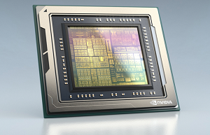
It All Starts With Design Files
Every board begins life as a digital plan. Engineers create layouts using design tools such as Altium Designer or Eagle, mapping out copper traces, component placements, and layers. On screen, it looks neat and logical. In reality, small choices can cause big headaches later.
Before fabrication begins, files go through design rule checks. These spot issues like traces that are too thin or spacing that feels a bit optimistic. This stage often feels slow, but skipping it is like building furniture without checking the measurements. Problems only show up when it is far too late.
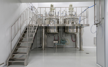
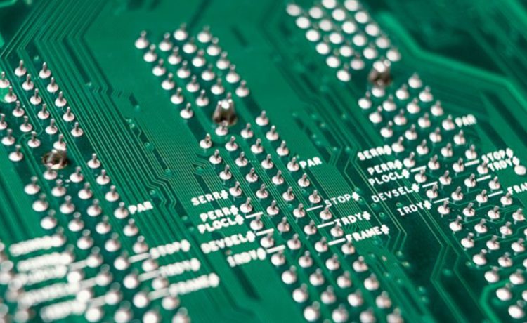
From Copper Sheets To Real Boards
Once designs are approved, the physical work begins. Copper-clad laminates are cut to size, cleaned, and prepared. The circuit pattern is transferred onto the board using imaging processes, followed by chemical etching that removes unwanted copper.
This is where PCB Fabrication in Singapore shows its strength. Local facilities tend to follow strict process controls, partly due to industry expectations and partly due to climate realities. Humidity, for example, affects materials more than many people expect, so careful handling makes a real difference.
After etching, layers are pressed together if the board is multi-layered. Holes are drilled for components and vias, then plated to ensure electrical connections run smoothly through the board.
Solder Mask, Silkscreen, And A Bit Of Personality
With the copper work done, boards move on to finishing steps. A solder mask is applied, usually green but sometimes red, blue, or black. It protects copper traces and reduces the risk of accidental short circuits.
Next comes the silkscreen. This adds component labels, reference numbers, and logos. It might seem cosmetic, but clear markings save hours during assembly and repair. Anyone who has tried troubleshooting an unlabelled board knows the frustration.
At this point, the board finally looks familiar. Flat, neat, and quietly confident.
Testing Before Anything Leaves The Floor
Before boards are approved, they are tested. Electrical testing checks for open circuits and shorts. Visual inspections catch alignment issues or surface defects. For higher-stakes applications, extra checks may be added.
Many companies working with electronic manufacturing services in Singapore value this stage the most. It reduces failure rates downstream and protects brand reputation. A faulty board rarely fails quietly. It usually fails at the worst possible time.
Why Local Manufacturing Still Matters
Global supply chains are useful, but they are not always flexible. Local production offers faster feedback, easier communication, and fewer surprises. When timelines are tight or designs change mid-project, proximity helps.
This is why electronic manufacturing services in Singapore remain relevant across industries, from industrial automation to consumer electronics. The mix of technical skill, process discipline, and regional experience is hard to replace.
From Board To Finished Product
Once fabrication is complete, boards move on to assembly. Components are placed, soldered, and tested again. Although fabrication and assembly are separate stages, they are closely linked. A well-made board simplifies everything that follows.
Understanding PCB Fabrication in Singapore helps teams design smarter, troubleshoot faster, and plan production more realistically. It also leads to better conversations with suppliers, which is often half the battle.
Conclusion
PCB fabrication is not just a technical process. It is a quiet collaboration between design intent and manufacturing reality. From the first layout file to the final inspection, every step leaves a mark on performance and reliability.
For businesses relying on electronic manufacturing services in Singapore, understanding how boards are made brings clarity and confidence. It turns production from a black box into a shared process.
To ensure reliable results and smooth production cycles, contact MPN Tech and discuss how their services can support your next project.